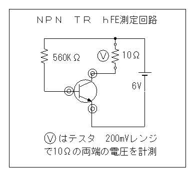
To match Transistors in hFE under similar condition to the usage in the amplifier, with up to 0.1 A of Ic, I found that I can’t rely on cheap hFE testers with limited current. I googled and found several easy ways to measure Transistor’s hFE. I was about to start with very simple circuit using only two resisters like this. This should be sufficient for my purpose of hFE matching, but I had thought I could make it a little better.
http://ph7dc.but.jp/dc_amp/hfe_sokutei.htm
At first, I found most popular idea as “Base current fixed” method. It fix Ib and read Ic. To control the Ib, using fixed voltage source with Zenner Di, and switch the resister value seems standard. Transistor Tester to test Hfe and working of NPN and PNP Transistors
However, I started wondering if it’s straightforward to adjust the Base current to make the environment of the Transister like real usage. In the end the collector current or Emitter current should be adjusted to Bias current of target circuit, but it’s affected by hFE a lot while tuning Base current. Instead of that, shouldn’t we set the Collector current and then measure the Base current theoretically? Probably there were several reasons why the “fixed Base current method” became popular, as below.
- It’s worried to measure very low Base current, such as a few μA.
- Larger Collector current means higher hFE, straight forward to understand.
- It’s possible to read out hFE figure directly in measuring voltage with mV unit across resister above Collector, when the Base Current and resister were set properly. It sounds very convenient.
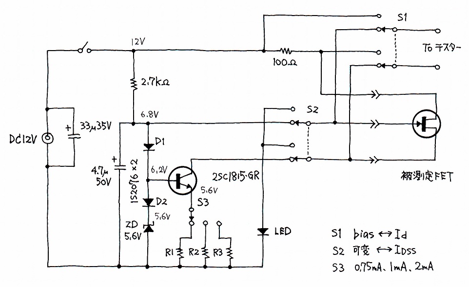
The former point shouldn’t be problem with modern high accuracy (High impedance) DMMs. The second reason is atractive, but I decided to do calculation of Ic/Ib everytime althouth I have to admit it’s troublesome. BTW I didn’t understand how the Collector current could be fixed (still don’t know), but the most of circuit with title “fixed Collector current” actually uses fixed Emitter method, so I also would go that route. There are some schematics to realize that idea, but the most of them are rather complicated. Below circuit design stands up from them showing simple smart idea. This is FET measurement device and not Transistor measurement design, but I believe we can put Tr in the place of FET so that fixed Emitter current can be pulled out from Tr. I think I haven’t seen same idea used for Transistor tester circuit. http://www.op316.com/tubes/toy-box/tester2.htm
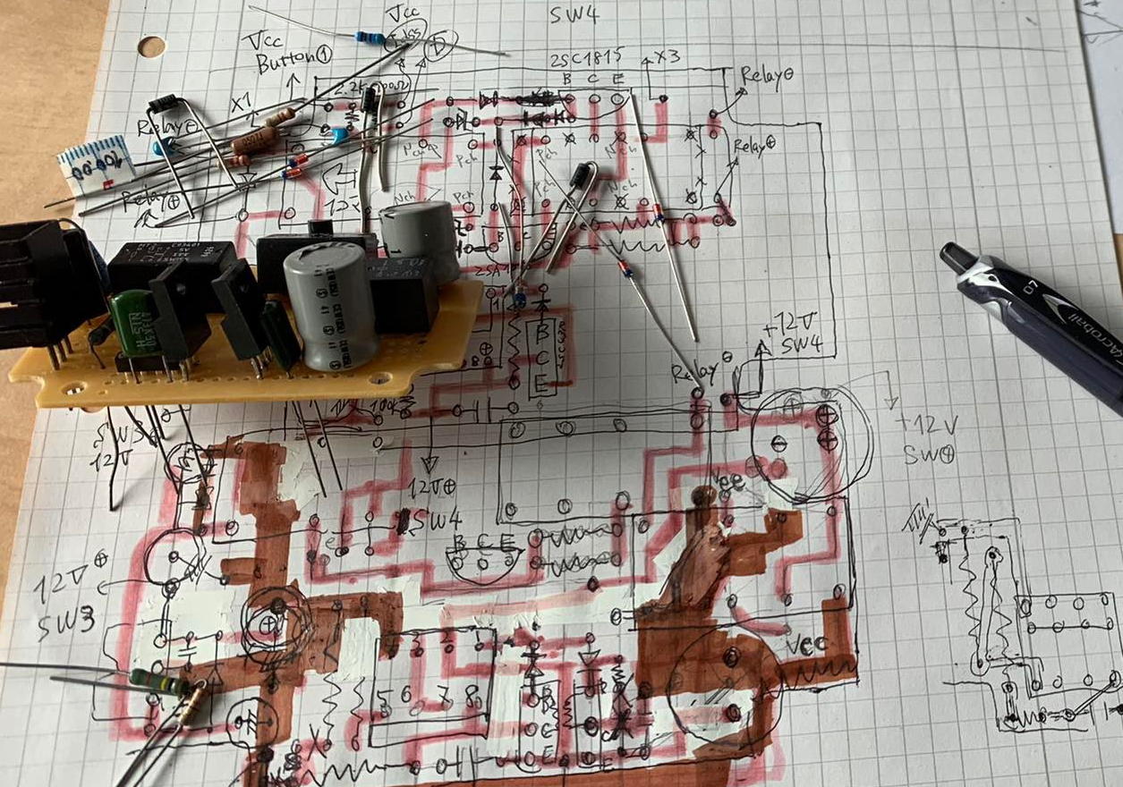
I ran some LTSpice simulations and could never exclude temp dependency of Zener and DUT’s Vbe even with compensation by attached Di. Then I found idea to use external fixed voltage source instead of Zener Di. Looks good. As many of you, I have a DC power supply box with so-so good stability. Why do we have to create “constant DC voltage source” inside of hFE tester? So I populated many components on the perfolated board in referring to this web page. I have many old OPamp, Trs, R, C in my box. I don’t need to be afraid of complexity of the circuit. Including voltage splitter and 3 relays for NPN/PNP switching and Tr/FET switching made the board full, as attached picture.
Project 177
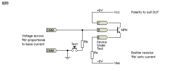
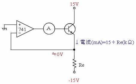
Right before starting soldering, I recognized that still I can’t be free from the influence of DUT’s Vbe variation and temperature dependency. Then I encountered a smart idea to include DUT inside of the OPamp’s Feedback loop. It achieves absolutely constant voltage on Re so that constant Ie can be realized. Also now the circuit became much simpler than before. This web page tells that this is originally idea from famous amplifier designer Mr. Kaneda.
Transistor, FET matching adapter
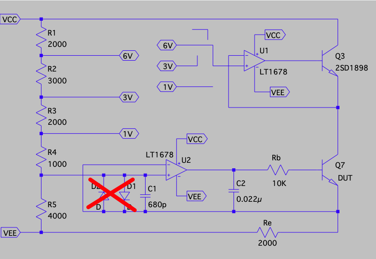
The original circuit by this web site owner contained full of protection features that can avoid any issues by any operation mistake. I tried to omit the most of them except some Caps with assumptions of “The voltage won’t exceed 4V”, “I never switch ON without DUT” and “synching connection switching by relay avoid mis-connection”. I drastically modified the power supply limiting the voltage on Re to only 4V. So the voltage distribution became asymmetric. Actually I wanted to use 12 V power supply on my shelf. And I hired one demand: variation of the measurement voltage in addition to the variation of the emitter current. Please see attached LT Spice screenshot. Now I can check Tr Hfe with 1, 3 and 6 volt on DUT. Emitter current can be set to any value by Re adjustment for 4V of VRe. PNP/NPN switching can be done by swapping VCC/VEE connection to the circuit and switching voltage controlling Tr between NPN/PNP. I can use this to measure Vgs of FET with constant Source current, by measuring the voltage between Gate and Source, too. IDSS measurement on Re is also possible by shortening Gate and Source while disconnecting the OP amplifier from DUT. If I want to measure with pulse current to avoid heating up DUT, probably I can add PWM circuit to U1 OPamp input. The input voltage limiting Di pair added for protection did nothing wrong on Simulation, but they disturbed this circuit working when I built it. Probably it was natural as Di makes Re and R5 parallel, then lower the OP amplifier input voltage significantly. I still don’t get why it worked on LTSpice, though.
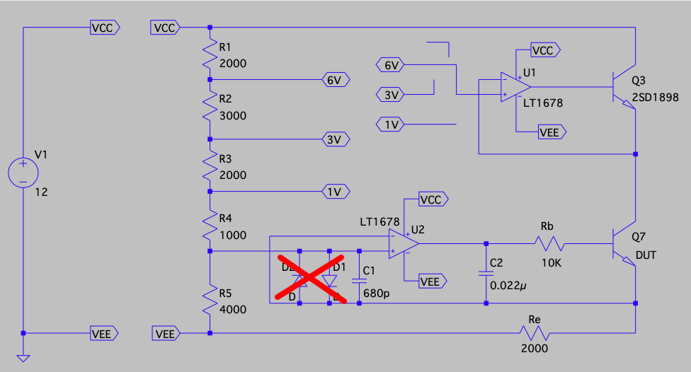
As you might realize already, I can’t design a new circuit at all. All what I did was just copy and paste from existing circuits on web. I appreciate very much to the experts who shares their know-how and idea of schematics on Internet. So I’m not sure if I’m doing right. It worked on LTSPice, and it seems working when I built. So your review of attached LTSpice screenshot is appreciated. If you find any critical mistakes, I’d happy to hear it. Thanks.


Comment